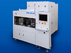


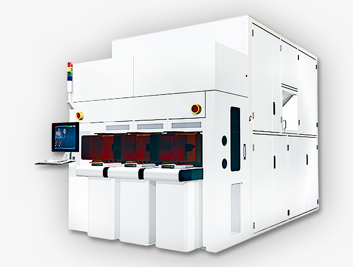
Nanosecond laser annealing system
 PRODUCTS
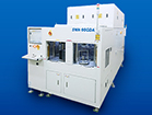
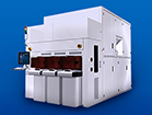
Laser System
PRODUCTS
Laser System
ITEM INFO
SUB-MICROSECOND MELT ANNEALING ACHIEVES ONLY WAFER SURFACE HEANTING
LT-3100 is an advanced laser annealing system designed to overcome the technical limitations that have traditionally challenged thermal processing for cutting-edge semiconductor devices. With its proprietary UV laser technology, LT-3100 enables highly controlled melt-based treatments ideal for dopant activation, thin-film crystallization, defect repair, surface smoothing, and 3D stacking applications.
The system achieves ultra-fast temperature ramp-up and ramp-down cycles of under 200 nanoseconds. Its step-and-repeat architecture ensures exceptionally uniform processing across any wafer size, including small-diameter power device wafers and ultra-thin wafers below 40 µm, making it an ideal solution for a wide range of advanced device manufacturers.
Equipped with a sophisticated real-time monitoring function, LT-3100 provides precise visibility into laser process behavior, supporting both stable mass-production operation and application-specific optimization.
For process development, the system features a unique tool that allows hundreds of process conditions to be applied to a single wafer simultaneously. This capability dramatically reduces the time and cost required for evaluating and optimizing processing parameters.
POINT
Product FeaturesPICK UP
- Ultra-low thermal budget
- High activation by melt-annealing
- Sub-micro second annealing
- Full device exposure
- High throughput
- Applicable to a variety of applications